When evaluating printed circuit board options, the distinction between single-sided and double-sided designs is often oversimplified to a matter of component density. The common assumption is that a second layer merely offers more real estate. This view misses the fundamental engineering leap that a two-layer board represents. The true advantage isn’t just about adding space; it’s about re-architecting the board’s entire electrical environment to achieve superior performance and reliability.
The secret lies in dedicating an entire layer to a single function: the ground plane. This strategic decision transforms the PCB from a passive component holder into an active system that manages signal integrity, mitigates interference, and improves thermal stability. Understanding the strategic advantages of double-sided PCBs is crucial for any project where performance is not negotiable.
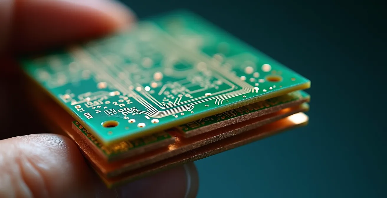
The Performance Blueprint of a Double-Sided PCB
This article deconstructs why a two-layer design is more than just an upgrade. We explore how a dedicated ground plane is the key to unlocking superior signal integrity by minimizing interference. We also detail how intelligent layout improves thermal management and component partitioning, ultimately delivering a higher project ROI despite a marginal increase in initial cost.
The Hidden Penalties of Forcing Complexity onto a Single Layer
Attempting to fit a moderately complex circuit onto a single-sided board often creates a “routing nightmare.” Without a second layer for connections, designers must use long, meandering traces and even physical wire jumpers to navigate the board. These lengthy paths act as unintentional antennas, making the device highly susceptible to picking up and radiating electromagnetic interference (EMI), which compromises its electromagnetic compatibility (EMC).
This inefficient routing creates large current return loops. Instead of a short, direct path back to the ground source, the current is forced to travel a circuitous route, which has a direct, negative impact on signal integrity. In mixed-signal designs, this can lead to “ground bounce,” where the ground reference voltage becomes unstable, corrupting both analog and digital signals.
Crosstalk Impact in Single Layer Designs
As detailed in a technical overview, crosstalk happens when signals on closely routed traces unintentionally interact. This problem occurs not only with side-by-side traces but also with traces routed in parallel on adjacent board layers, a phenomenon known as broadside coupling. Without a ground plane to shield them, adjacent traces on a single-layer board are prime candidates for this performance-degrading signal leakage. Source.
The most significant drawback of a single layer is the inability to implement an uninterrupted ground plane. This deficiency directly leads to increased crosstalk, where the electromagnetic fields from one trace induce unwanted noise in an adjacent one. For instance, high-frequency design best practices dictate that trace lengths must be strictly controlled, as 350 MHz bandwidth signals require traces under 10mm to avoid transmission line effects—a target that is nearly impossible to meet on a crowded single-layer board.
The visual result of these compromises is a board that looks chaotic and congested. The underlying electrical and physical stress is just as severe, leading to compromised performance from the start.

This congested layout isn’t just an aesthetic issue. The high component density and lack of thermal pathways put immense physical and thermal stress on the board. This often results in higher operational temperatures, which reduces the long-term reliability of components and the product as a whole.
| Metric | Single-Sided PCB | Double-Sided PCB |
|---|---|---|
| Routing Capacity | Limited to one layer | 2x routing area available |
| Signal Integrity | Poor at high frequencies | Better impedance control |
| Component Density | Low | 50%+ higher density possible |
| EMI Performance | High susceptibility | Reduced with ground plane |
Unlocking Superior Signal Integrity: The Ground Plane’s Strategic Role
The single greatest advantage of a double-sided PCB is the ability to dedicate an entire layer as an uninterrupted ground plane. This creates a ubiquitous, low-impedance return path for every signal on the board. Instead of current finding a convoluted path back to its source, it flows directly through the plane underneath the signal trace, dramatically improving electrical performance.
What is the main benefit of a ground plane?
The main benefit is creating a low-impedance return path for all signals, which drastically reduces electromagnetic interference (EMI) and improves overall signal integrity.
A ground plane acts as a shield, reducing EMI by providing a low-impedance path for return currents. This prevents the currents from forming large loops that radiate electromagnetic fields.
– Anonymous, ALLPCB
This solid ground plane minimizes return path loop areas, which directly mitigates EMI and enhances EMC. It’s a foundational element for designing high-speed digital interfaces like USB or Ethernet, where controlled impedance is critical. Designing traces with a specific impedance is far more predictable and effective when they are placed over a consistent ground plane. For example, following the 3W spacing rule (where the distance between traces is three times the trace width) reduces crosstalk by 70% in high-frequency PCBs, a guideline that is much easier to implement with a solid ground reference.
This concept can be visualized as a signal trace floating cleanly above a solid copper sheet. The ground plane provides a stable and predictable environment, shielding the signal from external noise and preventing its own fields from interfering with other parts of the circuit.

To connect this system, vias are used strategically to link components on the top layer directly to the ground plane below. This technique, known as “via stitching” when applied along the board edge, effectively walls off the circuit from external interference and ensures every component has a stable voltage reference, minimizing system-wide noise.
| Parameter | Without Ground Plane | With Solid Ground Plane | Improvement |
|---|---|---|---|
| Return Path Impedance | High (>50Ω) | Low (<5Ω) | 90% reduction |
| EMI Radiation | Significant | Minimal | 20-30dB reduction |
| Signal Rise Time | Degraded | Preserved | 2x better |
| Crosstalk | -20dB | -40dB or better | 100x improvement |
From Component Density to Design Intelligence: How Strategic Layout Drives Performance
With a two-layer design, component density becomes a tool for design intelligence, not just a way to fit more parts. Higher density enables miniaturization, which naturally leads to shorter trace lengths. For high-frequency signals, shorter traces mean less signal degradation, lower susceptibility to noise, and inherently better performance.
Double-sided PCBs not only support more complex designs but can also be more compact. Designers have more flexibility in routing, and the double-sided nature also lends to improved signal integrity.
– PGF Technology Group, PCB Design Analysis Report
This design freedom allows for logical partitioning. Sensitive analog components can be placed on one side of the board, while noisy digital components (like microcontrollers and switch-mode power supplies) are placed on the other. Each zone can have its own dedicated grounding scheme, preventing digital noise from corrupting analog measurements.
The elegant organization of a double-sided board reflects an engineered system where every component placement is deliberate. This clean layout contrasts sharply with the forced compromises of a single-layer design, leading to a more robust and predictable final product.
Beyond signal management, the second layer is a powerful tool for thermal management. Large copper pours can be connected directly to heat-generating components using thermal vias. This effectively turns a large portion of the PCB into a built-in heat sink, drawing heat away from critical ICs and improving the product’s overall reliability and lifespan. This intelligent layout ultimately simplifies the design process, drastically reducing the chance of discovering performance issues late in development that would require costly redesigns.
High-Density Layout Checklist
- Choose materials with a dielectric constant below 4 for reduced signal distortion.
- Implement differential pair routing for noise reduction in high-speed signals.
- Maintain continuous return paths with via stitching at a pitch between λ/20 and λ/10.
- Use thermal vias for components generating more than 2W of heat.
- Place analog and digital sections in separate zones with dedicated grounding.
| Strategy | Benefit | Application |
|---|---|---|
| Top: Digital, Bottom: Analog | Noise isolation | Mixed-signal designs |
| Heavy components top side | Assembly reliability | Power supplies |
| RF sections isolated | Signal integrity | Wireless devices |
| Thermal zones separated | Heat management | High-power circuits |
| Critical signals internal | EMI protection | High-speed digital |
Key Takeaways
- The true value of a double-sided PCB is its ability to host a dedicated ground plane.
- A solid ground plane is the most effective tool for improving signal integrity and reducing EMI.
- Two layers enable intelligent partitioning of components and superior thermal management.
- The initial cost increase of a double-sided PCB is often offset by reduced debugging time and higher reliability.
Evaluating the True ROI: Why Double-Sided Designs Can Lower Total Project Cost
A common objection to double-sided PCBs is the perceived higher cost. However, a true return on investment (ROI) analysis must look beyond the per-unit manufacturing price. The small upfront increase is often dwarfed by the significant savings in engineering time spent debugging complex routing, signal integrity, and EMI problems that plague single-layer designs.
Is a double-sided PCB always more expensive?
While the upfront manufacturing cost is slightly higher, double-sided PCBs often lower the *total project cost* by reducing debugging time, preventing costly redesigns, and improving long-term reliability.
A more robust and reliable design from the start leads to a faster time-to-market. This acceleration is frequently a more significant financial factor than the board’s cost, especially in competitive markets. The enhanced reliability also has long-term financial benefits. A board with better thermal and electrical characteristics will experience fewer field failures, leading to lower warranty claims and product support costs over its lifetime. The improved performance of double-sided PCBs is a direct investment in brand reputation and customer satisfaction.
Double-Sided PCB ROI Analysis
An industry analysis highlights that the cost savings associated with double-sided PCBs can be significant, particularly when producing large-scale projects. By utilizing double-sided PCBs, businesses can reduce their production costs and maximize their profits, especially when factoring in the total cost of ownership. Source.
Furthermore, scaling up production dramatically changes the cost equation. For example, volume orders of 1000+ units reduce per-board cost by 90% compared to prototypes, making the difference between single and double-sided boards negligible. The decision framework is clear: once signal frequencies rise above a few MHz, or when mixed-signal components are involved, a double-sided PCB is no longer an option but a requirement for project success. To realize these benefits, it is essential to find a reliable PCB manufacturer who can execute these complex designs with precision.
| Factor | Single-Sided Impact | Double-Sided Impact | ROI Benefit |
|---|---|---|---|
| Board Size | 100% baseline | 40-60% reduction | Lower material cost |
| Debug Time | Extended (poor SI) | Reduced (better SI) | Faster development |
| Field Failures | Higher rate | 50% reduction | Lower warranty costs |
| Redesign Risk | High | Low | Avoid respins |
| Production Yield | 85-90% | 95-98% | Less waste |
Frequently Asked Questions on PCB Performance
When does double-sided assembly become cost-effective?
When component density requires board size reduction of 40% or more, the savings in PCB material costs typically offset the additional assembly charges.
What’s the typical cost difference for double-sided assembly?
Double-sided assembly adds approximately $0.10-0.20 per board in volume production, but can save $2-5 per board in reduced PCB size.
How do double-sided designs affect time-to-market?
Despite slightly longer assembly times, double-sided designs often reduce overall development time by simplifying routing and eliminating redesign cycles.